
Description
Product Overview
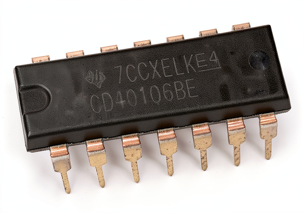
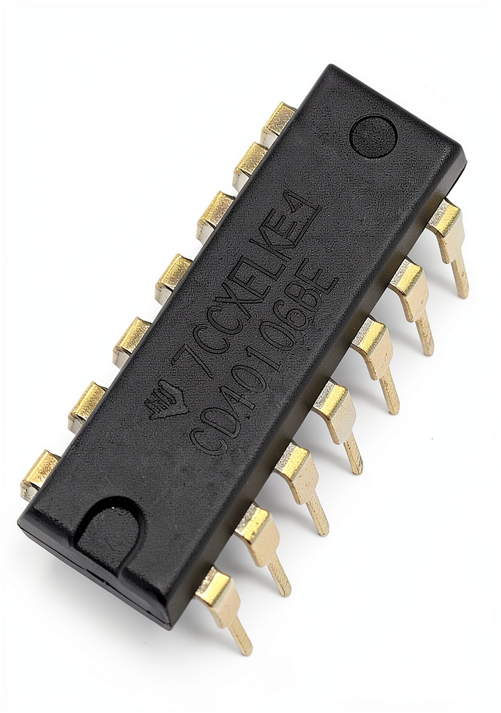
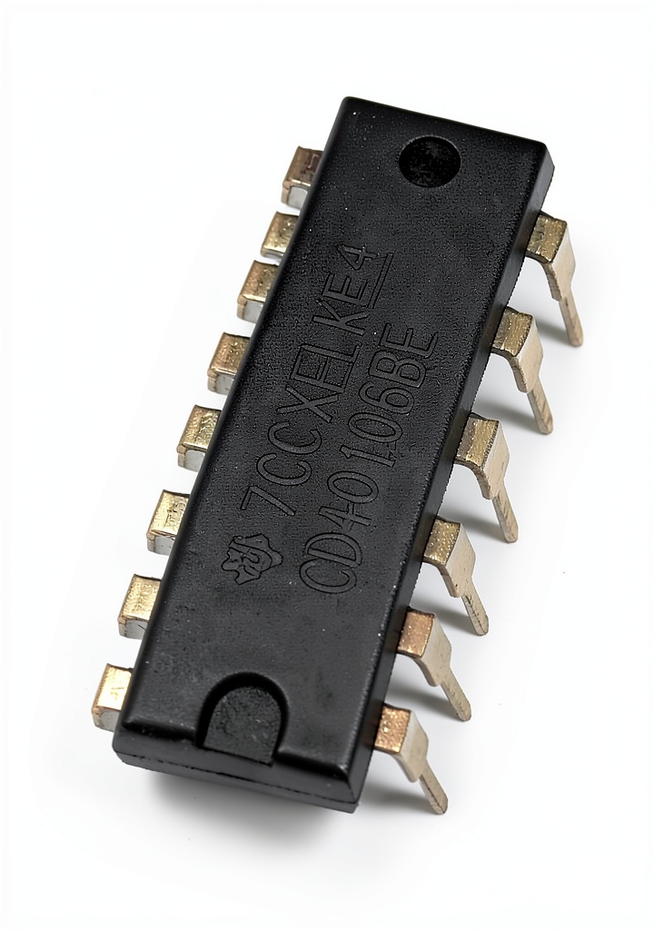
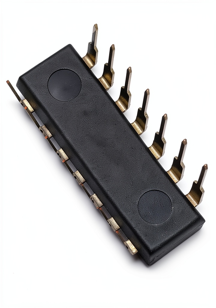
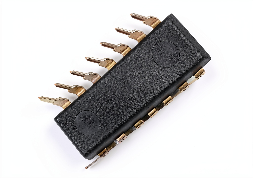
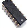
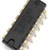
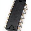
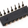
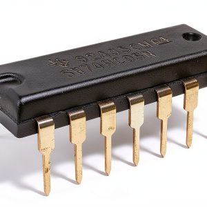
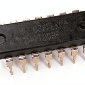
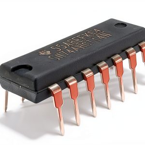
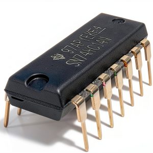
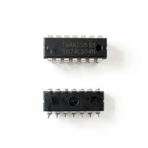
The CD40106BE from Texas Instruments is a CMOS hex Schmitt‑trigger inverter designed for demanding industrial and scientific applications. Each package contains six independent inverting gates, each featuring built‑in hysteresis that provides superior noise rejection and clean signal transitions. The device operates over a wide supply voltage range from 5 V to 15 V, making it adaptable to both low‑voltage logic families and higher‑voltage control circuits. With a typical hysteresis voltage of 0.9 V at 5 V supply, 2.3 V at 10 V, and 3.5 V at 15 V, the CD40106BE ensures that noisy or slowly changing inputs are reliably converted to crisp digital outputs.
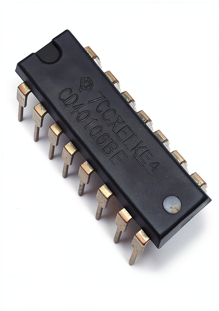
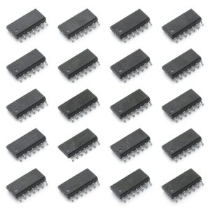
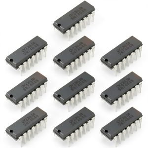
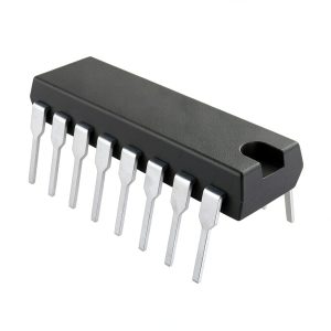
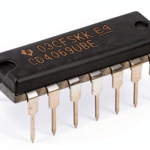
Key specifications include a maximum input current of 1 µA at 18 V, a quiescent current of less than 100 nA at 18 V and 25 °C, and a guaranteed low VDD and VSS current even during slow input ramps. The device tolerates any input rise or fall time, eliminating the need for external timing components in many designs. Packaged in a standard 16‑pin DIP or SOIC format, the CD40106BE is supplied in a convenient pack of 20, providing ample inventory for production runs and prototyping projects.
![[Product front view showing all components]](https://www.advex.store/wp-content/uploads/2026/08/922f90b6b75746409746c7e1393344b6.jpg)
Usage
Engineers and designers frequently employ the CD40106BE in environments where signal integrity is critical. Typical use cases include debounce circuits for mechanical switches, waveform shaping for pulse‑width modulation, and level‑shifting between different logic families. Its robust noise immunity makes it ideal for automotive sensor interfaces, industrial control panels, and laboratory instrumentation where electromagnetic interference is common.
Because the inverter tolerates a wide range of input rise and fall times, it can be used directly with slow‑moving sensors such as thermistors, photoresistors, and capacitive touch elements without additional buffering. The low power consumption enables battery‑powered devices to operate for extended periods, while the high noise immunity ensures reliable operation in harsh environments like factories, outdoor installations, and aerospace test rigs.
When integrating the CD40106BE into a PCB layout, keep the supply pins decoupled with a 0.1 µF ceramic capacitor placed close to the VDD pin. This simple step further improves transient response and reduces the likelihood of supply‑induced glitches. The device’s symmetrical output characteristics also simplify board routing, as each gate can drive both high‑side and low‑side loads without additional level‑shifting components.
Why Choose Us
Choosing the CD40106BE from Texas Instruments means selecting a component backed by decades of semiconductor expertise and a global support network. TI’s rigorous quality assurance processes guarantee that every unit meets or exceeds the specifications listed in the datasheet, providing confidence for mission‑critical applications.
Our distribution channels ensure fast, reliable delivery of the 20‑pack configuration, reducing lead times and inventory costs for manufacturers. In addition, we offer comprehensive technical documentation, reference designs, and application notes that help engineers accelerate development and troubleshoot any issues quickly.
Beyond the product itself, we provide responsive customer support, including access to TI’s worldwide engineering teams. Whether you need assistance with circuit design, thermal analysis, or compliance testing, our experts are ready to help you achieve optimal performance and reliability.
We also stand behind our products with a robust warranty and return policy, giving you peace of mind that your investment is protected. When you purchase the CD40106BE from us, you receive not only a high‑quality component but also a partnership dedicated to your success.
Key Features
- Six independent Schmitt‑trigger inverters provide reliable signal conversion with built‑in hysteresis.
- Wide supply voltage range (5 V‑15 V) supports diverse system requirements and reduces component count.
- Low quiescent current (<100 nA) extends battery life for portable and remote applications.
- High noise immunity (>50 %) ensures stable operation in electrically noisy environments.
- Comprehensive technical support and fast delivery of 20‑pack units for streamlined production.
FAQ
What is the typical hysteresis voltage for the CD40106BE?
The device exhibits a typical hysteresis voltage of about 0.9 V when powered at 5 V, 2.3 V at 10 V, and 3.5 V at 15 V, providing strong noise rejection across its operating range.
Can the CD40106BE handle slow input signal transitions?
Yes. The inverter has no limit on input rise and fall times, making it suitable for interfacing with slow sensors such as thermistors, photoresistors, and capacitive touch devices without additional buffering.
What packaging options are available for the CD40106BE?
The part is offered in standard 16‑pin DIP and SOIC packages, and it is sold in a convenient pack of 20 units, which is ideal for both prototyping and volume production.
How does the low power consumption benefit my design?
With a quiescent current of less than 100 nA at 25 °C, the CD40106BE minimizes overall system power draw, extending battery life for portable devices and reducing heat generation in dense electronic assemblies.
Is there technical support available for designing with the CD40106BE?
Absolutely. Texas Instruments provides extensive application notes, reference designs, and direct engineering assistance to help you integrate the inverter into a wide variety of applications efficiently.





























































Reviews
There are no reviews yet.