
Description
Product Overview
The CD4069UBE is a high‑performance CMOS hex inverter designed by Juried Engineering for demanding electronic projects. Each IC contains six independent inverting gates, providing a versatile solution for logic level conversion, signal conditioning, and timing adjustments. The device operates over a wide supply voltage range, typically 5 V to 15 V, and delivers typical propagation delays of 30 ns at a 10 V supply, ensuring rapid response in high‑speed circuits.
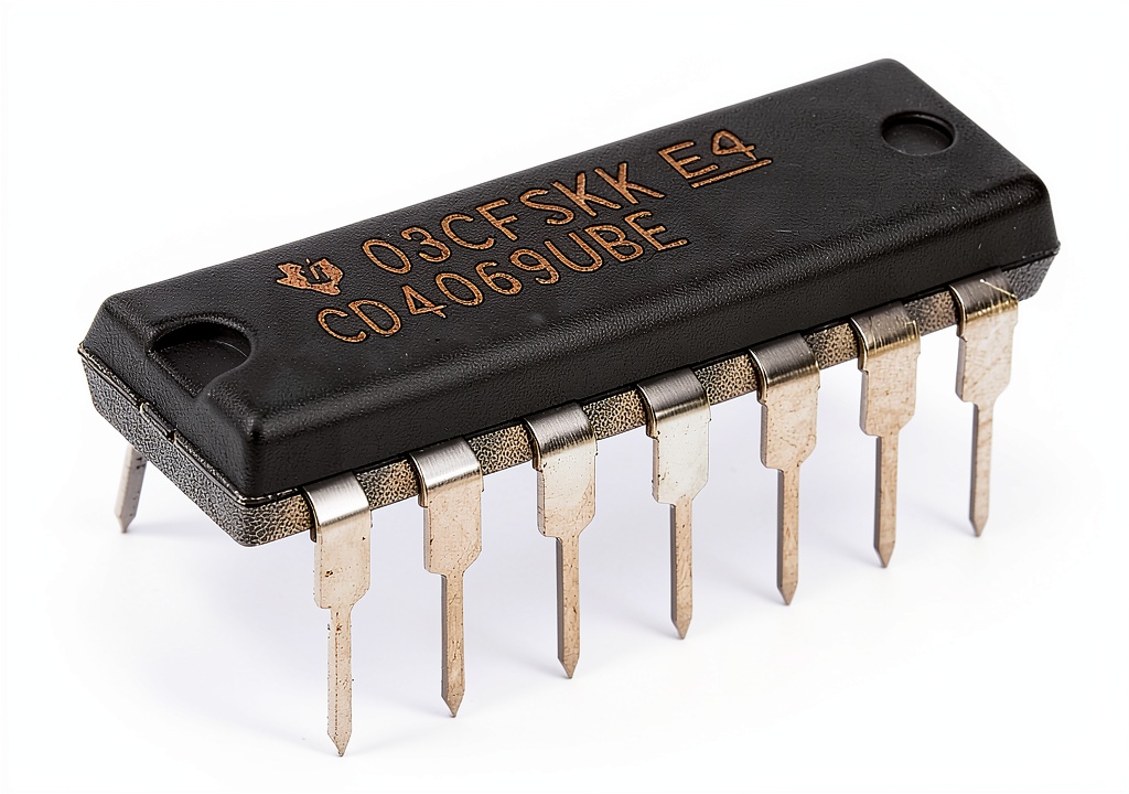
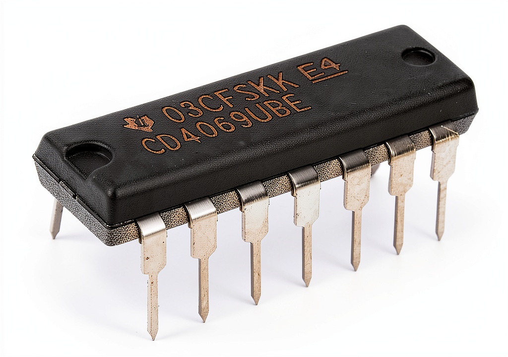
Built on a standard DIP‑14 package, the CD4069UBE is breadboard‑friendly, allowing engineers and hobbyists to prototype quickly without the need for specialized sockets. The pins are arranged in a familiar configuration, with each inverter gate occupying two adjacent pins, simplifying wiring and reducing the chance of errors during assembly. The package also offers excellent thermal characteristics, dissipating heat efficiently even under continuous operation.
One of the standout specifications of this component is its exceptionally low input current. Measured at 1 µA at 18 V across the full temperature range, and as low as 100 nA at 18 V and 25 °C, the CD4069UBE minimizes loading on preceding stages, preserving signal integrity and extending battery life in portable applications. This low quiescent current also contributes to reduced overall power consumption, a critical factor in modern low‑power designs.
Reliability is further reinforced by rigorous testing. The IC meets the JEDEC tentative standard No. 13B for B‑Series CMOS devices, guaranteeing that each unit conforms to industry‑wide expectations for voltage tolerance, temperature stability, and electrical performance. The result is a component that can be trusted in both laboratory environments and field‑deployed systems.
In addition to its technical merits, the CD4069UBE is supplied in a convenient pack of ten, providing ample inventory for production runs, educational labs, or extensive prototyping efforts. The consistent quality across the pack ensures that every unit behaves identically, simplifying design verification and reducing the need for individual part testing.
Usage
Designers frequently employ the CD4069UBE in applications that require precise logic inversion with minimal delay. Typical use cases include pulse shaping circuits, where the inverter cleans up noisy edges and creates well‑defined transitions for downstream components. Its fast propagation time makes it suitable for clock‑divider networks, where timing accuracy directly impacts system performance.
Oscillator circuits benefit from the CD4069UBE’s ability to provide stable feedback with low distortion. By integrating the inverter into a resonant tank circuit, engineers can generate reliable square‑wave outputs for timing references, microcontroller clocks, or audio‑frequency generators. The low input current ensures that the oscillator’s amplitude remains consistent, even when powered from limited sources.
High‑input‑impedance amplifiers often require a buffer stage to prevent loading effects. The CD4069UBE serves as an excellent buffer, offering high input impedance while delivering a clean inverted output. This characteristic is valuable in sensor interfaces, where the source signal must be preserved without degradation.
Beyond these core applications, the inverter finds utility in educational settings, where students explore fundamental digital logic concepts. Its robust construction and clear pinout make it an ideal teaching tool for labs focused on Boolean algebra, truth tables, and gate-level design. The pack of ten ensures that multiple groups can work simultaneously without resource constraints.
In industrial environments, the CD4069UBE can be incorporated into safety‑critical systems that monitor signal polarity and trigger alarms when abnormal conditions arise. Its reliable operation across a broad temperature range (‑55 °C to 125 °C) guarantees performance in harsh conditions, from automotive control units to outdoor instrumentation.
Why Choose Us
Juried Engineering has a long history of delivering semiconductor components that meet stringent quality standards. The CD4069UBE benefits from this legacy, offering a product that has undergone 100 % testing for quiescent current at the maximum rated voltage of 20 V. This thorough validation process eliminates variability and ensures that every unit performs within the specified parameters.
Our commitment to customer satisfaction extends beyond the product itself. We provide comprehensive technical documentation, including detailed pinout diagrams, recommended operating conditions, and application notes that guide users through common design challenges. This support reduces development time and helps engineers achieve optimal results faster.
When you purchase the CD4069UBE pack of ten, you receive a consistent batch that has been screened for defects, guaranteeing that each IC behaves identically. This uniformity is essential for large‑scale production runs where part‑to‑part variation can lead to costly rework or system failures.
In addition to the product, we offer responsive after‑sales service. Our technical support team is available to answer questions about integration, troubleshoot unexpected behavior, and provide recommendations for complementary components. This level of assistance ensures that you can rely on the CD4069UBE throughout the entire lifecycle of your project.
Finally, our competitive pricing and reliable shipping logistics mean that you receive high‑quality components on schedule, enabling you to meet tight project deadlines without compromising on performance.
Key Features
- Fast 30 ns typical propagation for high‑speed digital circuits
- Ultra‑low input current reduces loading on preceding stages
- DIP‑14 package is breadboard‑friendly and easy to prototype
- Meets JEDEC B‑Series standards for reliability across temperature ranges
- Comes with dedicated technical support and comprehensive documentation
FAQ
What voltage range can the CD4069UBE operate within?
The device is designed to function reliably from 5 V up to 15 V, covering most low‑power and standard logic supply levels. It also tolerates higher voltages up to 20 V for short periods, making it versatile for a variety of circuit designs.
How does the low input current benefit my circuit?
Low input current means the inverter draws minimal power from the signal source, preserving signal integrity and extending battery life in portable applications. This characteristic is especially important when interfacing with high‑impedance sensors or delicate analog front ends.
Can the CD4069UBE be used in high‑temperature environments?
Yes. The component is rated for operation from –55 °C to 125 °C, ensuring reliable performance in automotive, industrial, and outdoor applications where temperature extremes are common.
Is the pack of ten suitable for production runs?
Absolutely. The ten‑unit pack provides a consistent supply of tested parts, reducing the need for individual part verification and streamlining inventory management for medium‑scale manufacturing projects.
What support resources are available if I encounter integration issues?
Juried Engineering offers detailed datasheets, application notes, and a responsive technical support team. You can contact our engineers for guidance on schematic design, layout considerations, and troubleshooting any unexpected behavior.
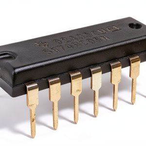

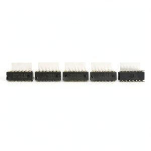
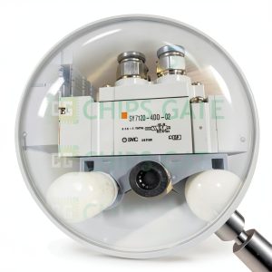
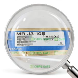 MR-J3-10B Inverter Logic Gate New in Box – CG Chips Gate – 1 Piece
Reviews
There are no reviews yet.