

Description
Product Overview
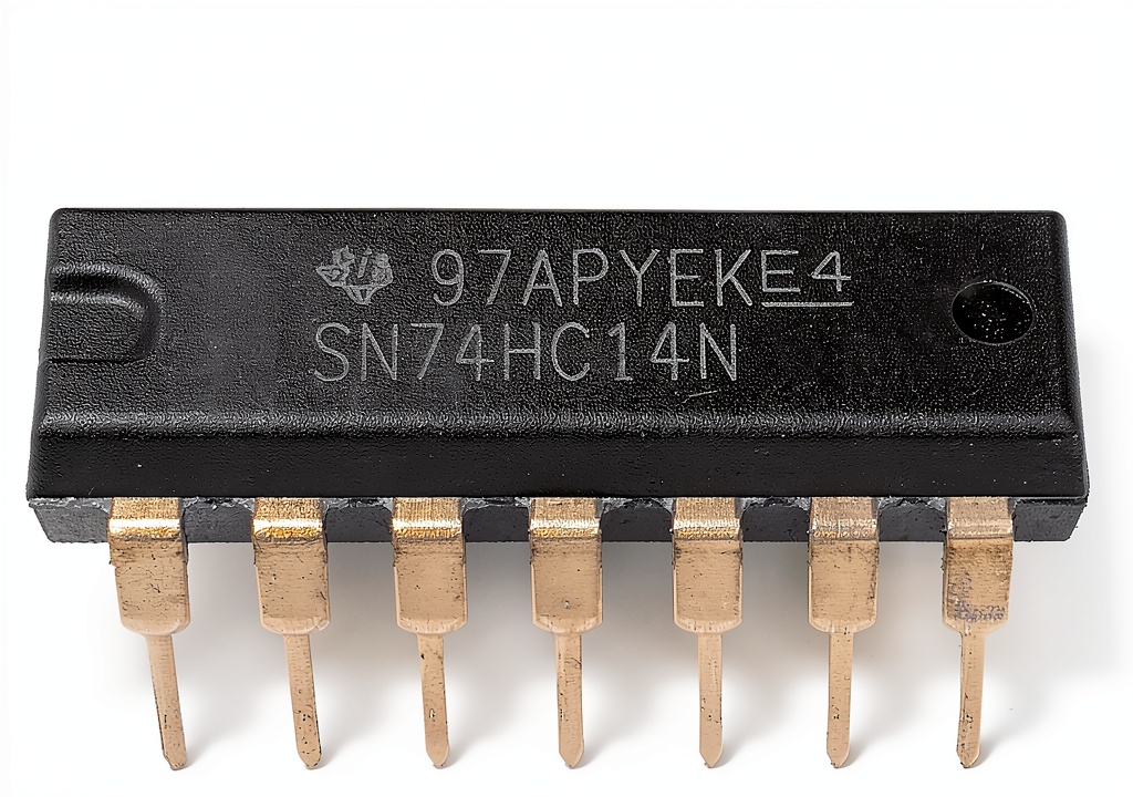
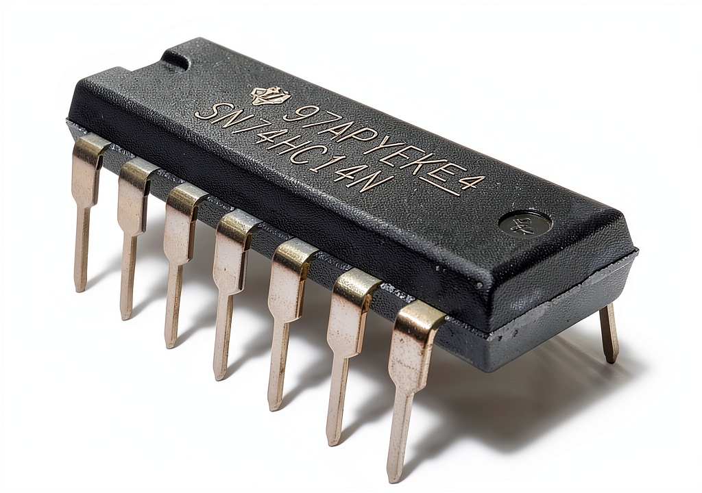
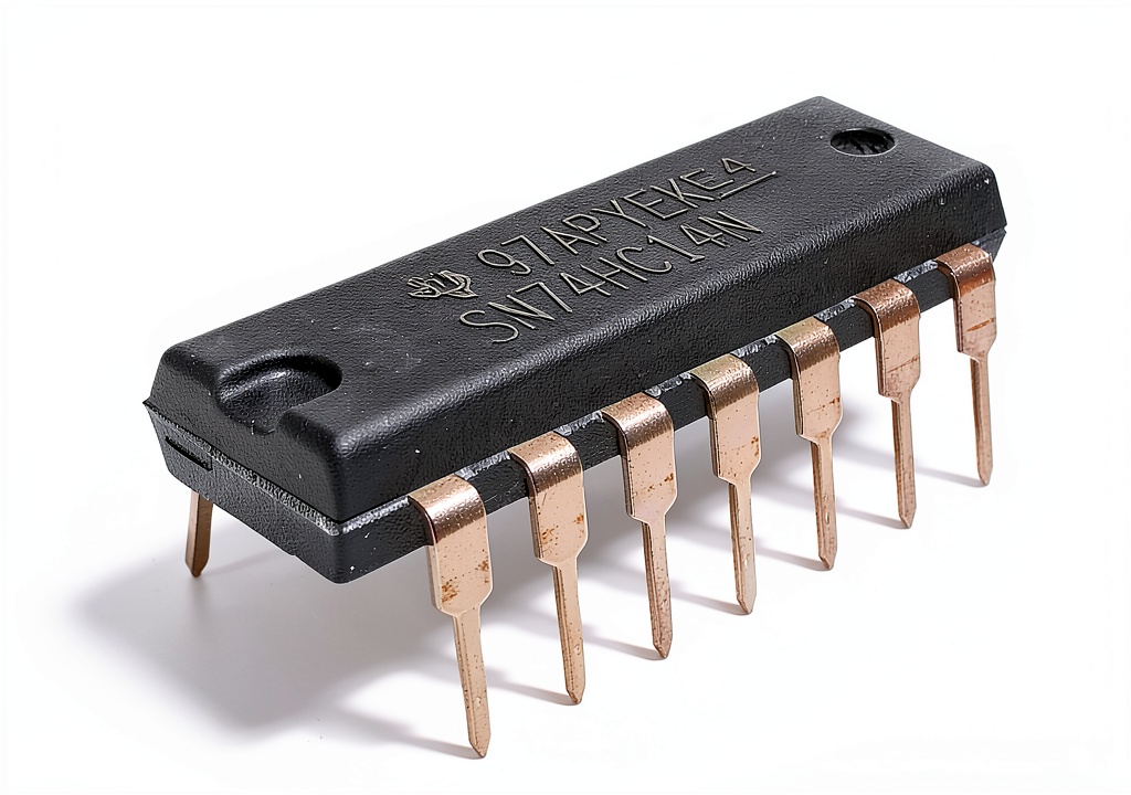
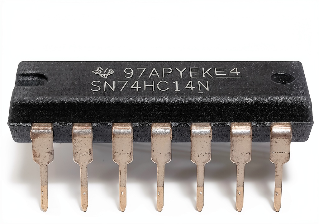
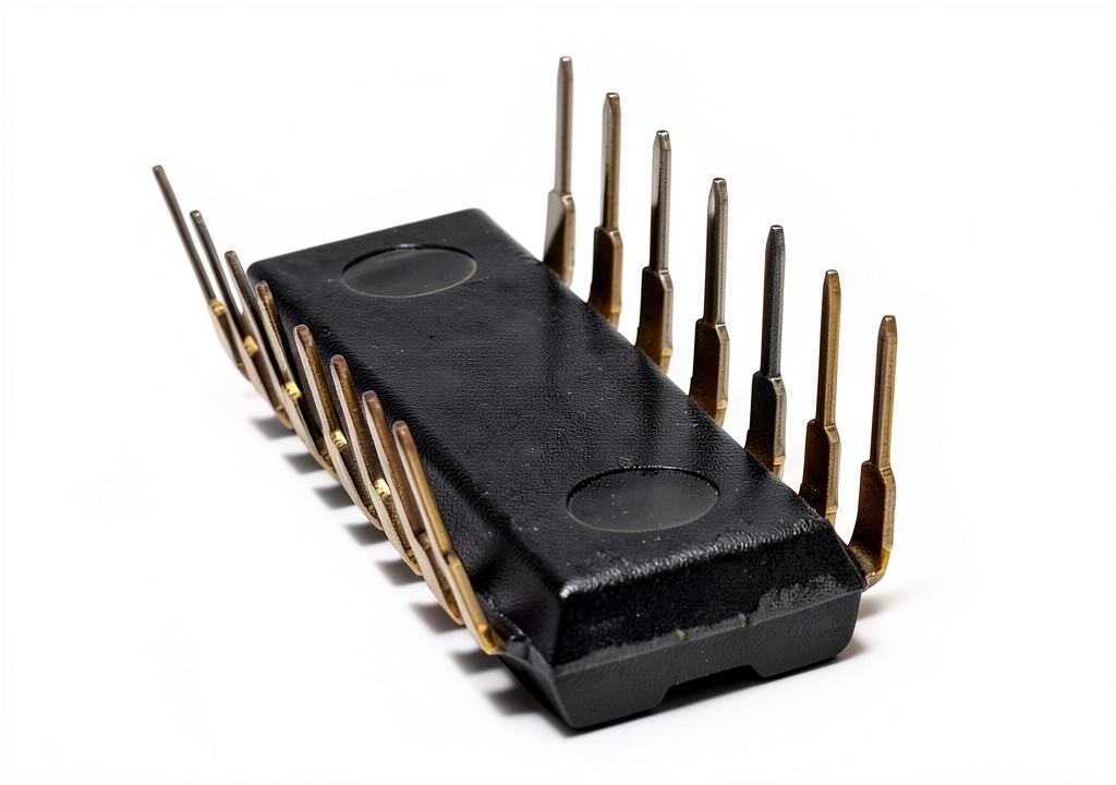
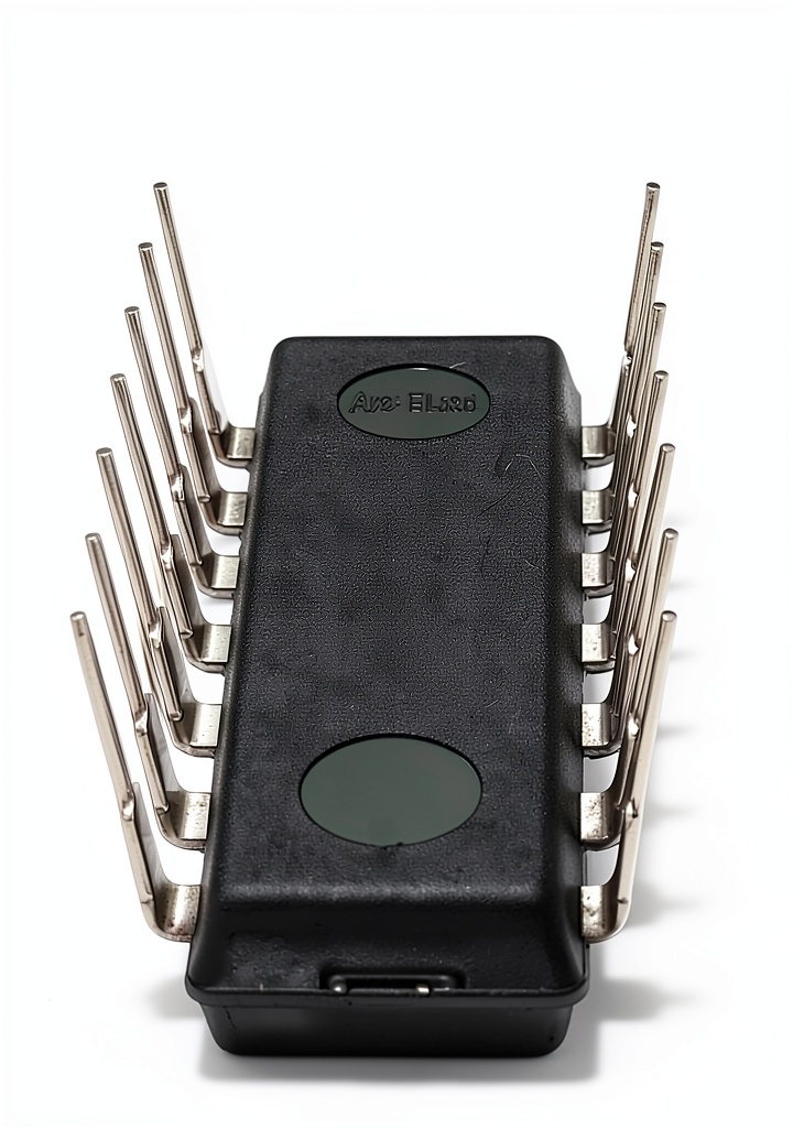
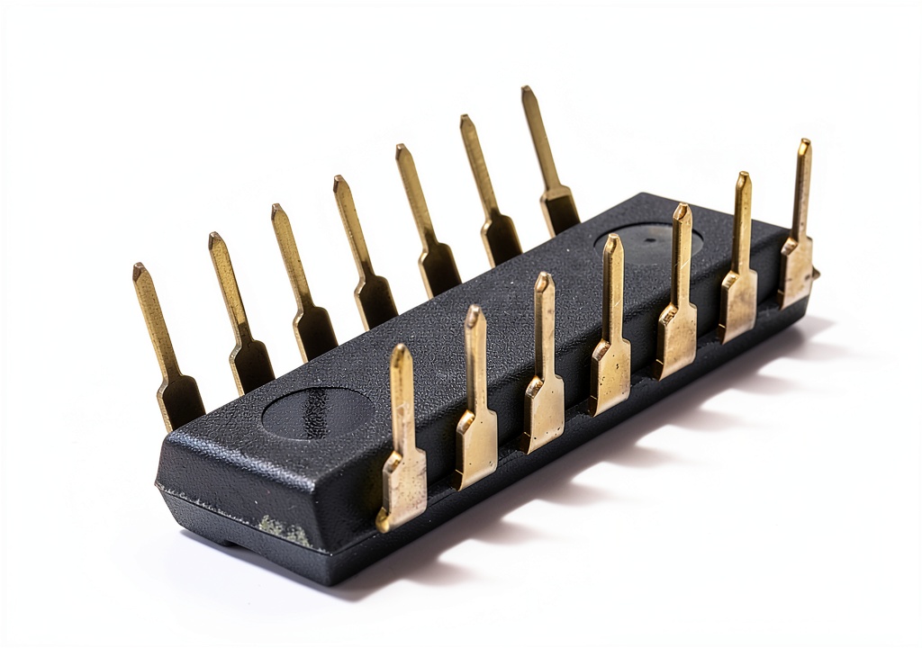
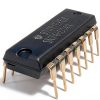
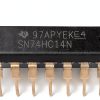
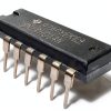
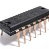
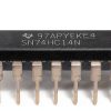
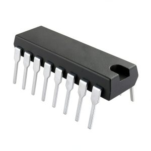
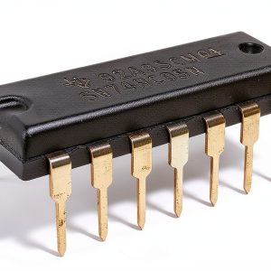
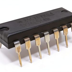
The SN74HC14N is a high‑performance hex Schmitt‑trigger inverter manufactured by Texas Instruments, presented in a convenient DIP‑14 package that fits easily onto standard breadboards and prototype boards. Each device contains six independent inverters, each equipped with a Schmitt‑trigger input that provides hysteresis, reducing noise susceptibility and ensuring clean digital transitions. The part operates over a wide supply voltage range of 2 V to 6 V, making it suitable for both low‑voltage microcontroller environments and higher‑voltage logic families.
Designed for low power applications, the IC draws a maximum supply current of only 20 µA (ICC) and an input leakage current of just 1 µA, which helps extend battery life in portable designs. Despite its low power profile, the SN74HC14N can source or sink up to ±4 mA at a 5 V supply, allowing it to drive up to ten LSTTL loads per output. The typical propagation delay is 11 ns, delivering fast response times that are essential for high‑speed digital circuits.
Each inverter channel is protected against over‑voltage conditions and includes built‑in ESD protection, contributing to the overall reliability of the component in demanding industrial and scientific applications. The device’s robust construction and consistent performance have earned it a strong reputation among engineers who require dependable logic conversion in compact form factors.
![[Product front view showing all components]](https://www.advex.store/wp-content/uploads/2026/07/72272d8c7f3f452bbe3df92ba7414a75.jpg)
Usage
The SN74HC14N finds use in a broad spectrum of electronic projects and professional designs. Its Schmitt‑trigger inputs make it ideal for cleaning up noisy signals from mechanical switches, sensors, and low‑level analog sources before they enter digital logic. Engineers often employ the device in edge‑detect circuits, pulse‑stretching applications, and as part of oscillator or timing circuits where precise threshold control is required.
Because of its wide operating voltage range, the IC can be integrated into battery‑powered devices, handheld instrumentation, and low‑power IoT modules. The ability to drive multiple LSTTL loads means it can serve as an interface between modern CMOS logic and legacy TTL systems, facilitating seamless communication across different technology generations.
In educational settings, the DIP‑14 footprint simplifies hands‑on learning for students exploring digital logic fundamentals. The six independent inverters allow multiple experiments to be conducted on a single chip, reducing component inventory and cost for teaching labs.
Why Choose Us
When selecting a Schmitt‑trigger inverter, reliability, performance, and support are paramount. Texas Instruments, a globally recognized leader in semiconductor manufacturing, guarantees that each SN74HC14N unit meets stringent quality standards and undergoes comprehensive testing before shipment. Our distribution network ensures rapid delivery, and our technical support team is ready to assist with design queries, layout recommendations, and troubleshooting.
We provide detailed datasheets, application notes, and reference designs that help engineers accelerate development cycles. Our commitment to sustainability means the ICs are produced using environmentally responsible processes, and we offer recycling programs for end‑of‑life components.
Choosing the SN74HC14N means investing in a component that combines low power consumption, fast switching, and robust drive capability—all backed by the reputation of Texas Instruments and our dedicated customer service.
Key Features
- Six independent Schmitt‑trigger inverters provide noise‑immune signal conversion.
- Wide supply voltage range of 2 V to 6 V supports diverse power environments.
- Low static power draw (20 µA max) extends battery life in portable designs.
- Can drive up to ten LSTTL loads per output, enabling legacy TTL interfacing.
- Backed by TI’s global support and comprehensive design resources.
FAQ
What is the typical propagation delay of the SN74HC14N?
The device exhibits a typical propagation delay of about 11 ns, which ensures rapid signal transition for high‑speed digital applications.
Can the SN74HC14N operate from a single 3.3 V supply?
Yes, the IC is fully functional across the 2 V to 6 V range, so a 3.3 V supply is well within its operating specifications.
How many loads can each inverter output drive?
Each output can source or sink up to ±4 mA at a 5 V supply, allowing it to drive up to ten LSTTL loads reliably.
Is the SN74HC14N suitable for battery‑powered projects?
Absolutely. Its low supply current (20 µA max) and low input leakage (1 µA) make it an excellent choice for battery‑operated devices where power efficiency is critical.
What protection features are built into the device?
The IC includes internal ESD protection and over‑voltage tolerance, helping to safeguard the component in harsh operating conditions.
 Cengage Learning Pulmonary Medicine 7th Edition Print Replica
Reviews
There are no reviews yet.